Sep. 16, 2020
Announcement of pilot testing service, non-destructive defect inspection for SiC epitaxial wafers
 As a consignment project of Ministry of Economy, Trade and Industry*1, Toray Research Center Inc. will conduct a consigned analysis service of SiC epitaxial wafer by non-destructive defect inspection for the purpose of the dissemination of the IEC International Standards*2. As part of this project, we will begin pilot testing service of non-destructive defect inspection of SiC epitaxial wafers using the defect inspection instrument (SICA88 manufactured by Lasertec Corporation) which is installed in National Institute of Advanced Industrial Science and Technology.
Taking this opportunity, please try out the defect-inspection method in compliance with IEC standards.

・The pilot test period is from October 1, 2020 to March 31, 2021 and the inspection will be provided for free during the period.
・This inspection is intended for the epitaxial layer with a thickness range of 10-30 um.
・Defect class identification is carried out using standard recipes for SiC epi-defect inspection in accordance with IEC standards.
・High defect recognition accuracy can be achieved by using a combined method of optical inspection and photoluminescence.

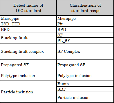
【Table 1 Correlation between defect names of the IEC standard and classifications of standard recipe】

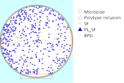
【Figure 1 In-plane distribution of main defects in 6 inch 4H-SiC epitaxial wafer】
 We are engaged in development of the SiC power-device industry as well as utilization and dissemination of international standards as a third-party organization.

*1 International Standardization and Dissemination Support Program for Energy Saving in the field of International Electrotechnical Commission (IEC)
*2 IEC Project Number:IEC 63068-1~3
Title:”Non-destructive recognition criteria of defects in silicon carbide homoepitaxial wafer for power devices”
Part 1:Classification of defects
Part 2:Test method for defects using optical inspection
Part 3:Test method for defects using photoluminescence


【Contact】
Please contact the following person in charge for any inquiries or foregoing announcement.

Keiichi Yamada
Surface Science Laboratory
Toray Research Center Inc.
e-mail : keiichi_yamada@trc.toray.co.jp